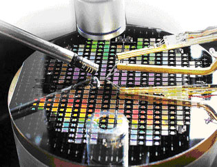
Along with the Optical MEMS technology that forms the core of AGM products, a number of other technologies play crucial roles in bringing AGM products to market and making sure they are effective and reliable in the field. Semiconductor Wafer Processing is one of these technologies. The fabrication of MEMS devices using Semiconductor Wafer Processing technology is significantly more challenging than the fabrication of traditional Integrated Circuits. Because of the deep etches involved, coupled with narrow dimensions and strict dimensional tolerances, MEMS fabrication demands special expertise from the Process and Design Engineers who carry it out. The experience that AGM engineers bring in the areas of lithography, etching, bonding, and metal deposition allows for effective and meaningful partnerships with MEMS foundries, ultimately leading to higher yields and lower costs for our customers. Automated testing, with high speed and good precision, is the other key technology that AGM has developed for testing ESVOA, 2D Micromirror MEMS, and other products.

In the realm of wafer and chip testing of Optical MEMS devices, a number of interrelated technologies come together to enable reliable and efficient testing. These include wafer probers, optomechanical fixtures, advanced optical measurement instruments, electronic and optical hardware, and customized test software using advanced algorithms. AGM has developed automated systems for testing MOEMS chips with high precision and high throughput. These test systems are often highly specialized, so that a different test station is used for testing each of AGM’s distinct products. For example, a different test station is used for AGM’s 2D Micromirror product, than the one used with AGM’s ESVOA product. There is another station for testing Mirror Array products. This specialized, multidisciplinary test capability is a key factor enabling AGM to bring Optical MEMS products to the market in a timely and reliable manner.